
Corona RP8D1 - Reverse Engineering
Due to my special interests in a customized RC transmitter and receiver system I started with reverse engineering of a Corona RP8D1 35MHz receiver.
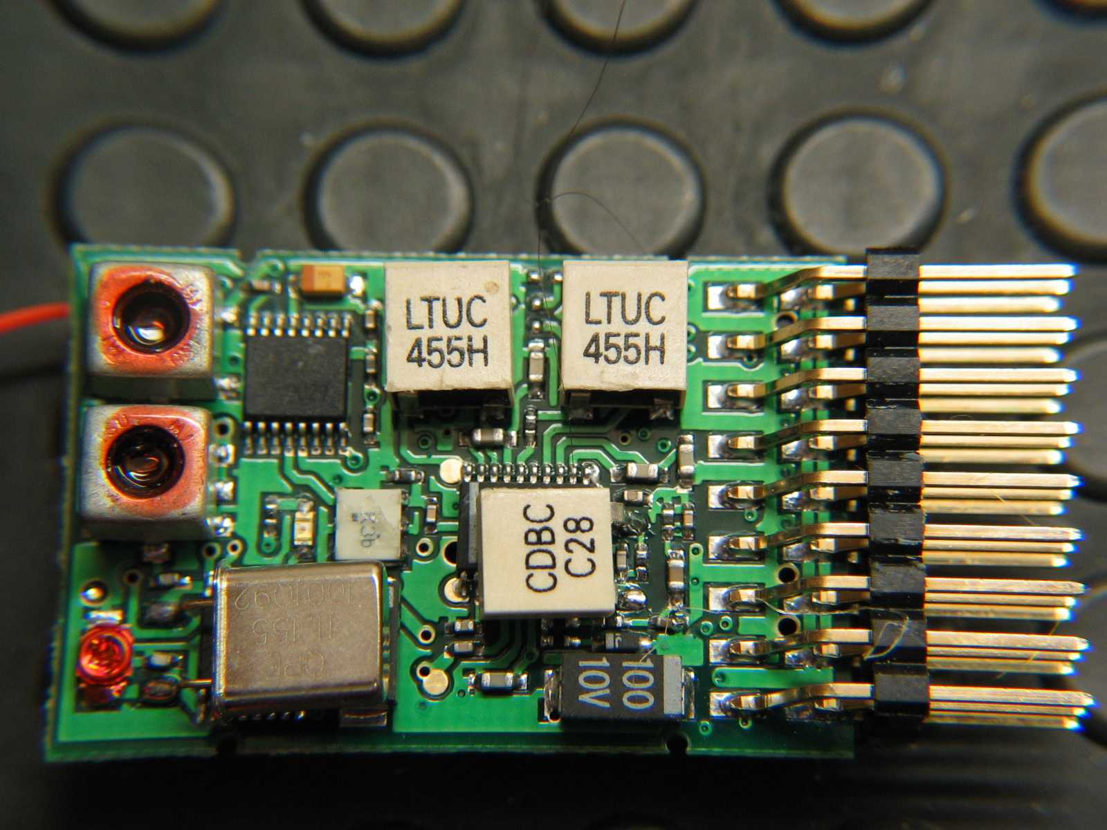
The RP8D1 is my favourite candidate cause it´s a double superheterodyne receiver, uses a PLL synthesizer and is controller by an AVR ATmega88V.
Interesting fact about the micro-controller:
Corona obviously has been changed the controller type on actual receiver boards. The first receiver I bought in mid 2010 uses the mentioned ATmega88V.
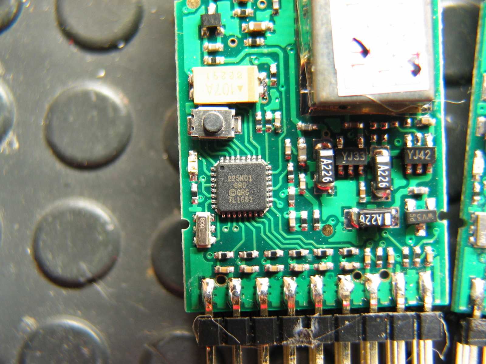
Two newer receiver, bought in January 2011, are using a controller marked "225K01" with manufacturer "QRG".
Fact is the PCB layout is 100% identical on both receivers so must be the pin-out of the different controllers!
So the 225K01 is either a clone or some official AVR derivative, already contacted Atmel for details.
Used components, followed by pictures and the controller pin-out:
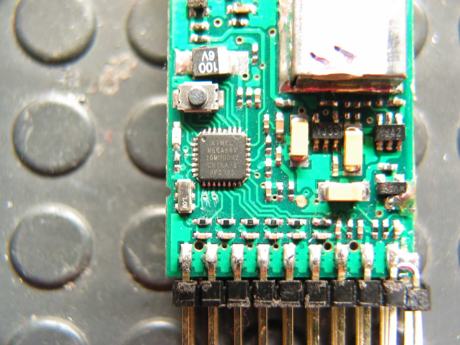
- Controller AVR ATmega88V on mid 2010 board
- Controller QRG 225K01 on 2011 boards
- Rohm BU2630 Dual PLL
- Rohm BH4126 Wideband IF Detector
- Philips SA616DK High Performance Mixer FM IF System
Board top layer:
Board top layer, filter and crystal removed:
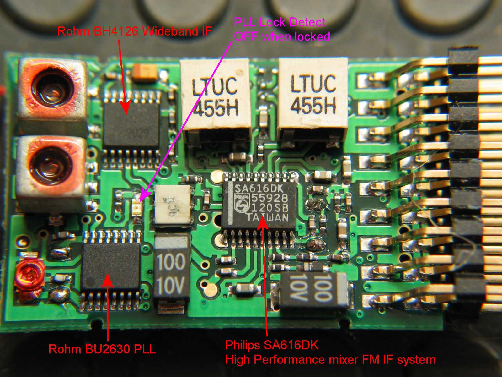
A word about the second LED (PLL lock detect) on the RP8D1: The LED will signal the status of the PLL control loop. If the LED lights the PLL is out of sync, that means the synthesizer can not set the receiving frequency correctly. For normal operation the LED shall be always off.
Board bottom layer:
There is a typo in the picture, the controller type is 225K01.
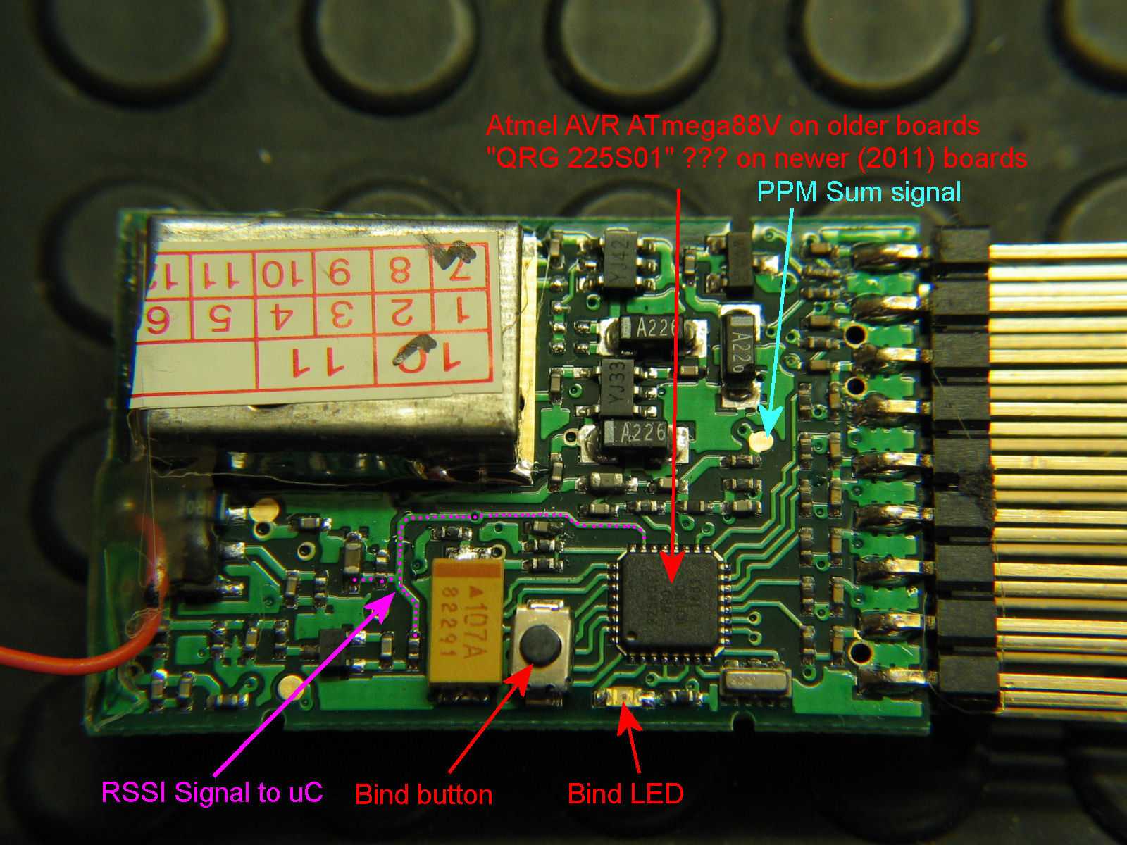
The RSSI signal can be picked up for external use easily on one of the resistors instead of removing the filter and wiring to the SA616 pin 5.
Receiver board with AVR ATmega88V controller:
Receiver board with QRG 225K01 controller:
Controller pin-out:
Pin	Name	Function
1	PD3	Bind button input
2	PD4	Bind LED output
3	GND	GND
4	VCC	VCC 3.3V
5	GND	GND
6	VCC	VCC 3.3V
7	XTAL1	Crystal 8MHz
8	XTAL2	Crystal 8MHz
9	PD5	Not connected
10	PD6/AIN0	PPM sum signal input
11	PD7/AIN1	DC 1.46V
12	PB0	Channel 1 PPM output
13	PB1	Channel 2 PPM output
14	PB2	Channel 3 PPM output
15	PB3	Channel 4 PPM output
16	PB4	Channel 5 PPM output
17	PB5	Channel 6 PPM output
18	AVCC	AVCC 3.26V
19	ADC6	Not connected
20	AREF	AREF 3.26V
21	GND	GND
22	ADC7	Not connected
23	PC0/ADC0	RSSI signal input
24	PC1/ADC1	PPM signal threshold for analog comparator, level set by ext. voltage divider

25	PC2	PLL CE signal output
26	PC3	PLL DATA signal output
27	PC4	PLL CLK signal output
28	PC5	Not connected
29	PC6	Channel 9 PPM output
30	PD0	Channel 8 PPM output
31	PD1	Channel 7 PPM output
32	PD2	Not connected
Unfortunately pin PC6, the RESET input, is used as IO pin, this means the ISP serial interface is disabled and one can´t dump the flash and EEPROM content. (Already tried ;-) ) Therefore only parallel programming is the way to go which is quite complicated due to the MLF package and required number of wiring connections.
I made a HV programming adapter and tried to dump the flash of the controller. Unfortunately the memory protection fuse is set, so that´s not an option.
The boot reset fuse isn´t set so there is no bootloader installed.
A fact: The QRG 225K01 is definately an ATmega88 since the signature bytes match in AVR-Studio.
Some more work to do. In any case a firmware for the AVR must be programmed from scratch.
👈 Home